Nanophotonics
Nanophotonics – Yet another innovation in Solar PV technology
Renewable energy has seen a huge growth in the past decades. The depletion of fossil fuels and global warming are the major reasons for this. Renewable energy sources are of wide range, some of the most prominent ones are solar power, hydropower, tidal power, wind power, nuclear power and so on. Among these, solar has become one of the most favorite sources among the researchers as well as companies. The various advantages of this technology is the major reason for this. This energy is green, includes very less alteration of the site, safe, has nearly no effect of ecosystem and also has many other advantages. As any other technology, this one has some demerits too. Cost of the energy is a major factor in solar energy. The efficiency of the generation should be increased to reduce the cost of energy. Researches have improved the technology to a large extent the previous decades. One among those improvements is the application of Nanophotonics to solar power generation. In this research paper, let us discuss about Nanophotonics in Solar power.
Solar power– A Brief overview:
Solar energy is about using the sun’s energy to generate electricity either directly or using the energy for heating applications. Solar radiation is harvested and converted into electricity by using photovoltaic cells. Photovoltaic cells produce electricity from electromagnetic radiation, usually light. Photovoltaic cells do not have any moving parts. They work on the principle of photovoltaic effect, the process by which voltage and current is generated in a solar cell (PV cell) when it is exposed to the sunlight.
PV cell construction and working:
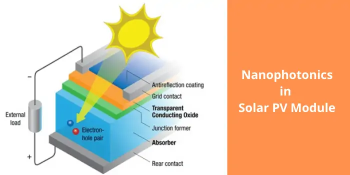
PV cells consists of a solar panel in which a p-type semiconductor and a n-type semiconductor, combined to form a p-n junction. The junction forms an electric field. The charged particles move across the junction. When sunlight, which is an electromagnetic radiation is focused on the solar panel, the photons in the light are absorbed by the semiconductor panel. The energy from these photons are transferred to the atoms of the semiconductor material. This energy is transferred to the electrons in the material. The electrons get excited to a higher energy level. This excitation of electrons in the presence of an electric field, causes the electrons move to the n-side, instead of the usual movement to p-side (opposite direction). The electron movement to n-side results in movement of holes (positive charges) to the p-side. This movement of charges in the presence of a electric field, results in the generation of electricity. The figure 1 Shows the construction and working of a PV cell

Figure 1. Photovoltaic effect; Working of a PV Cell
Challenges faced in solar power:
As any other technology, PV cells also have limitations. They are
- The Efficiency of the panels is as low as 15%. Losses are high throughout the energy conversion process
- The amount of sunlight trapped or absorbed by the panels is a major concern regarding the efficiency of the PV cell. Only 20 – 40% of the sunlight is being used by the PV panels, the rest is being wasted as heat.
Both the above limitations can be overcome by using suitable materials in solar panels. Such materials should absorb more sunlight and thereby give high output. Hence both cost and efficiency are not compromised. This is when ‘Nanophotonics’ comes into picture. Nanophotonics can be used to increase the efficiency of the panel in absorbing or trapping sunlight. Let us have a look at the concept of nanophotonics, principles and how it is useful in PV cells in the following sections.
Nanophotonics:
Nanophotonics is the branch of Optics that studies the properties of light at nanometer scale and also the interaction of nanometer-scale structures with light. Nanophotonics cannot be applied in conventional optical equipment, as light cannot be focused to nanometer scale normally. Special techniques are available for this purpose. The common types or principles of nanophotonics implementation are as follows:
- Plasmons and metal optics
- Near-field optics
- Metamaterials
Nanophotonics is finding applications in various fields like Microscopy, spectroscopy, optoelectronics and microelectronics. Other than these, it is now emerging as a boon in solar power generation. The application and achievement of nanophotonics in the field of PV cell is being discussed in the following sections. Figure 2 shows the market growth and size for applications targeted by nanophotonics.

Figure 2
Application of Nanophotonics in PV cells:
Nanophotonics helps us overcome the major challenges in PV cell technology, sunlight absorption by the panel and cost of the PV cell. Nanophotonics aims in reducing the size of the PV cells to the scale of nanometers and also increasing the light absorption at the same time. Conventional cells are large in size and absorb more light compared to thin cells. But the cost of the cell increases with size, as the material used increases with size.
Light trapping using Nanophotonics:
The theoretical limit for light absorption by a material is 4n2, where ‘n’ is the refractive index of the material. This is calculated by treating light as a straight ray. But capturing a light beyond its critical angle, can make the light captured inside the material for longer time, hence increasing the absorption of the light by the material. This is called light trapping. Light trapping in thin film PV cells is carried out using nano-photonics.
Increase light absorption in thin layer cells:
The amount of light photons absorbed by the semiconductor electrons, depends on the time given for the photons to interact with the material. The time taken for absorption depends on the refractive index and absorption coefficient of the material. The time pf propagation of light inside the material can be increased by light trapping.

Figure 3. Light trapping techniques
Light trapping is the phenomena which uses the effect of total internal refection between the semiconductor material and the surrounding medium. By increasing the roughness of the medium, the direction of the light propagation can be randomized.
Construction of Nanophotonic based light trapping Thin layer cells:
The construction of the thin film cells which use nano-photonics for light trapping is shown below in

Figure 4. Construction of thin film Nanophotonic PV cell
The topmost layer is the scattering layer which has Nano-size particles, the second layer is the cladding layer and the bottom most layer is a mirror layer for reflecting back the light rays. In between these three layers the absorption layer or the active layer is sandwiched.
Efficiency of the above design:
The absorption of this design of thin film cell in enhanced by 15 times, nearly 60n2. This stands as a proof that proper designing of a thin film cells using nanophotonic principles can help us increase the absorption efficiency of the cell and also reduce the size of the cells, thereby reducing the cost of the energy.
Design enhancements for further increase in efficiency:
The efficiency of thin film PV cell light trapping can be further increased by replacing the flat nano-particle scattering layer with nanocones and nanowires. The figure 5 shows the comparison of the absorption profiles of various nano-structures

Figure 5. Flat vs Nanowires bvs Nanocones aborption profiles.
Advantages of Nanophotonic light trapping
- Reduction in PV cell size
- Higher absorption efficiency
- Low cost of energy
- Easy implementation
Solar power is at its prime in this era of renewable energy. The renewable sector is investing a lot in the solar power. At this stage, a branch of study like Nanophotonics, which helps us to overcome the two big challenges of the solar PV cell generation, namely Cost and efficiency, is a boon to the Solar power sector. This phenomenon of Nanophotonics should be further studied by the solar power enthusiasts.
Nanophotonics is yet another feather in the hat of Solar energy.
PowernSun :
Powernsun provides provides solar products like solar PV modules, solar inverters, solar monitoring, solar inverter accessories, Micro Inverter and Optimizer, Fuel Save Controller, Monitoring & Control Systems, Solar Charge Controller, Solar Structures, Solar Cables, PV Combiner Boxes, solar PV Connectors, Cable Tray, Energy Storage System, Solar Street Light, Solar Pump Inverter, Solar Refrigerators & Freezers, Online & Line Interactive UPS, Access To Energy, Water Purifier with the main aim of increase value and energy result at low cost.
Contact us
Power n Sun:
Office Suite 3510, Burlington Tower,
Marasi Drive Business Bay, Dubai, UAE
Phone : +971 43686393
Email : info@powernsun.com
Useful Blogs
On Grid Solar System
Solar earnings show demand fears overblown
Time, Cost and Quality Dimension of Solar Projects
Off grid solar system
Hybrid solar system
How to choose solar panel system
Solar system for home
what is solar inverter and it types?
Advantages of using solar energy
How to increase solar energy efficiency using Solar inverter clipping


Leave a Reply